Today in collaboration with TSMC, ARM’s physical IP division is announcing the tapeout of a 10nm test chip demonstrating the company’s readiness for the new manufacturing process. The new test chip is particularly interesting as it contains ARM’s yet-to-be-announced “Artemis” CPU core. ARM discloses that tapeout actually took place back in December 2015 and is expecting silicon to come back from the foundry in the following weeks.
The test chip serves as a learning platform for both ARM and TSMC in tuning their tools and manufacturing process to achieve the best results in terms of performance, power, and area. ARM actually implemented a full 4-core Artemis cluster on the test chip which should serve as a representative implementation of what vendors are expected to use in their production designs. The test chip also harbours a current generation Mali GPU implementation with 1 shader core that serves as a demonstration of what vendors should expect when choosing ARM’s POP IP in conjunction with its GPU IP. Besides the CPU and GPU we find also a range of other IP blocks and I/O interfaces that are used for validation of the new manufacturing process.
TSMC’s 10FF manufacturing process primarily promises a large improvement in density with scalings of up to 2.1x compared to the previous 16nm manufacturing node. At the same time, the new process is able to achive 11-12% higher performance at each process’ respective nominal voltage, or a 30% reduction in power at the same frequency.
In terms of a direct comparison between a current Cortex A72 design on 16FF+ and an Artemis core on 10FF on the preliminary test chip with an early physical design kit (PDK) we see that the new CPU and process are able to roughly halve the dynamic power consumption. Currently clock frequencies on the new design still don’t reach what is achievable on the older more mature process and IP, but ARM expects this to change in the future as it continues to optimise its POP and the process stabilises.
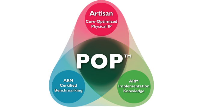
As manufacturing processes increasingly rise in their complexity, physical design implementation becomes an increasingly important part of CPU and SoC designs. As such, tools such as ARM’s POP IP become increasingly important for vendors to be able to achieve a competitive result both in terms of PPA and time-to-market of an SoC. Today’s announcement serves as demonstration of ARM commitment to stay ahead of the curve in terms of enabling its partners to make the best out of the IP that they license.
Source: anandtech.com